Skip to content
Are you tired of bulky, inefficient power adapters? These old designs often can’t keep up with modern electronics. Gallium Nitride (GaN) technology offers a massive leap forward.
GaN transistors dramatically improve power adapter efficiency and power density. They achieve this through superior electrical properties like high electron mobility, a wide bandgap, and low on-resistance. This means smaller, lighter, and faster-charging adapters for all your devices.
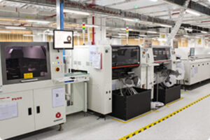
We’ve seen electronic devices get smaller and more powerful year after year. But often, the power adapters haven’t quite kept pace. As a company dedicated to power solutions, we at Quankang Technology have been deeply involved in this evolution. We understand the push for better performance. That’s why the advancements with GaN transistors are so exciting. Let’s dive into how these tiny components are making such a big difference in the world of power adapters. I believe understanding this can help product designers like Jacky make more informed choices.
What Electrical Superpowers Do GaN Transistors Bring To Power Adapters?
Struggling with the limitations of traditional silicon in your power designs? Silicon has served us well, but it’s hitting its limits. GaN transistors possess unique electrical characteristics that unlock new levels of performance.
GaN transistors excel because they have much higher electron mobility for faster switching, a wider bandgap allowing them to handle higher voltages, and significantly lower on-resistance, which cuts down energy loss and heat dramatically.
When we first started exploring GaN at Quankang, it was like discovering a new toolkit for power design. The fundamental properties of GaN are what give it such an edge over silicon, especially for the demanding applications we see today. For anyone involved in product design, like Jacky who focuses on balancing innovation and cost, understanding these core differences is key. Let’s break down these electrical characteristics.
The Magic of High Electron Mobility?
GaN transistors boast an electron mobility that’s about 1,000 times higher than what we see in traditional silicon-based transistors. What does this mean in practical terms? It means that for the same applied voltage, GaN devices can conduct a much higher density of current. This high electron mobility directly translates to a lower on-resistance (Rds(on)) when the transistor is switched on, especially in high-frequency switching power supplies. I remember when we first prototyped a GaN-based adapter; the reduction in conduction losses was immediately noticeable on our test bench. This ability to operate efficiently at higher frequencies also allows us to use smaller passive components, like transformers and inductors. For designers aiming for miniaturization without sacrificing power, this is a huge win. It opens doors to sleeker, more portable product designs, something I know Jacky values for consumer electronics.
Why is a Wide Bandgap a Game-Changer?
The bandgap of a semiconductor material is crucial for its electrical performance, particularly its ability to handle voltage. GaN has a bandgap width of approximately 3.4 electron volts (eV), which is significantly wider than silicon’s 1.1 eV. This wider bandgap allows GaN devices to withstand much higher electric fields before breaking down. This means GaN transistors can handle higher operating voltages, typically between 600V and 1200V.
This is a massive advantage for applications like industrial power supplies or the increasingly popular electric vehicle chargers we’re seeing. A higher breakdown voltage also means we can often simplify the external protection circuitry in our adapter designs, which can help reduce both complexity and cost. Furthermore, the wide bandgap results in lower leakage currents, even at high temperatures, contributing to better overall system efficiency and reliability. We’ve found this particularly beneficial in creating robust power solutions that need to perform reliably in tough conditions.
| Property | Silicon (Si) | Gallium Nitride (GaN) | Impact on Power Adapters |
|---|---|---|---|
| Electron Mobility | Lower | ~1000x Higher | Faster switching, lower conduction losses |
| Bandgap | ~1.1 eV | ~3.4 eV | Higher breakdown voltage, lower leakage |
| On-Resistance | Higher | Lower | Improved efficiency, less heat generation |
| Critical Field | Lower | Higher | Higher voltage operation, more compact design |
How Does Low On-Resistance Directly Boost Efficiency?
One of the most celebrated features of GaN transistors is their remarkably low on-resistance. This characteristic is directly linked to the high electron mobility we discussed earlier. Lower on-resistance means less power is wasted as heat when current flows through the transistor in its ‘on’ state. This reduction in conduction losses is especially significant in high-frequency switching operations, where the transistor is turning on and off millions of times per second. At Quankang, when we design an adapter, efficiency is always a top priority. Using GaN helps us push those efficiency numbers higher, often exceeding 90-95% in many applications. This directly translates to less wasted energy, lower operating temperatures for the adapter, and ultimately, improved reliability and a longer lifespan for the product. For end-users, this means a cooler adapter and potentially lower electricity bills. For designers like Jacky, it means meeting stringent energy efficiency standards like DOE VI more easily.
How Does GaN’s High-Frequency Capability Reshape Adapters, And What Are The Snags?
Are your power adapters still too big and clunky for modern devices? High-frequency operation shrinks them down. GaN makes this possible, but there are a few challenges to navigate.
GaN transistors can operate at much higher switching frequencies, often in the hundreds of kilohertz or even megahertz. This allows for significantly smaller passive components like transformers and inductors, leading to more compact and lightweight power adapters.

The ability to shrink power adapters without compromising performance is a constant goal in our industry. As a designer myself, I’ve seen firsthand how market demands push for smaller, lighter accessories, especially for portable electronics. GaN’s capability to operate at high frequencies is central to achieving this. However, pushing frequencies higher isn’t without its complexities. We need to consider the whole system.
The Freedom of High-Frequency Operation?
GaN transistors can switch on and off much faster than their silicon counterparts. We’re talking about operating frequencies in the range of hundreds of kilohertz (kHz) or even into the megahertz (MHz) spectrum. This is a leap from traditional silicon devices, which typically operate at lower frequencies. Why is this important? Because the size of key passive components in a power adapter, such as transformers and inductors, is inversely proportional to the switching frequency. So, by increasing the frequency, we can dramatically reduce the physical size and weight of these components. I recall a project where switching from a silicon-based design to a GaN-based one allowed us to reduce the adapter volume by nearly 40%. This size and weight advantage is incredibly valuable in markets for portable devices, smart home products, and even automotive applications where space is at a premium. For product managers like Jacky, this means more design flexibility for the end product.
What About the Heat in These Compact Designs?
While GaN transistors are more efficient and generate less waste heat compared to silicon, operating at high frequencies and high power densities still produces heat. The challenge is that this heat is now concentrated in a much smaller volume. If not managed properly, this can lead to overheating, reduced component lifespan, and even device failure. At Quankang, thermal management is a critical part of our GaN adapter design process. We often have to employ more sophisticated cooling solutions than what might be needed for a bulkier, lower-frequency silicon adapter. This can include carefully designed heat sinks, the use of thermal interface materials (TIMs) to improve heat transfer, or even active cooling in very high-power applications. It’s a balancing act; we want the smallest possible adapter, but we can’t sacrifice reliability. Jacky’s challenge of managing cost while ensuring performance is very relevant here – effective thermal management adds to the cost but is crucial for quality.
Are GaN Costs Still a Barrier?
Currently, the manufacturing process for GaN devices is more complex and less mature than the decades-old silicon fabrication processes. This results in a higher per-unit cost for GaN transistors. While the performance benefits are clear, this cost premium can be a barrier to adoption, especially in highly cost-sensitive consumer electronics segments. From my experience at Quankang, we’ve seen that while early adopters and high-performance niche markets are willing to pay for GaN’s advantages, broader market penetration requires cost reduction. The good news is that as GaN manufacturing technology matures and production volumes increase, we are seeing a steady decline in costs. I’m confident that in the coming years, GaN will become much more cost-competitive, making its superior performance accessible for a wider range of applications. We are already designing our next-generation platforms with GaN in mind, preparing for this shift.
| Aspect of High-Frequency GaN Operation | Advantage | Challenge | Our Approach at Quankang |
|---|---|---|---|
| Component Size | Significantly smaller transformers & inductors | N/A | Leverage for compact adapter designs |
| Power Density | Much higher W/cm³ or W/in³ | Heat concentration in smaller volume | Advanced thermal management strategies |
| Overall Adapter Size/Weight | Smaller, lighter, more portable | Potential for increased thermal stress | Balancing size reduction with reliability |
| Manufacturing Cost | (Indirectly, less material) | GaN transistor cost currently higher than Si | Monitor cost trends, design for future adoption |
In Which Real-World Applications Is GaN Technology Already Shining?
Is GaN just a lab curiosity, or is it actually making a difference now? You might be surprised. From the charger in your bag to critical infrastructure, GaN is already powering innovation.
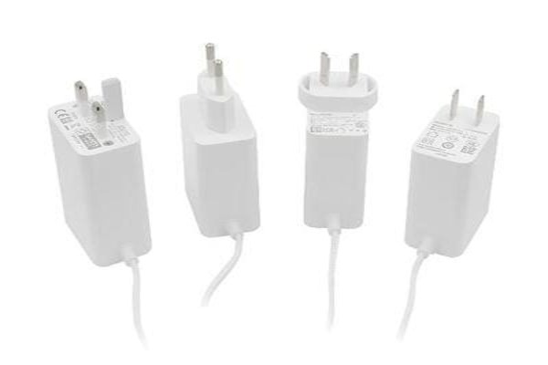
GaN technology is making a significant impact in fast chargers for smartphones and laptops, power management in data centers, and compact, efficient chargers for electric vehicles. Its benefits are tangible and widespread.
It’s one thing to talk about the theoretical benefits of a technology, but it’s another to see it in action. At Quankang, we’re not just experimenting with GaN; we’re actively incorporating it into solutions for various markets. The demand from clients like Jacky, who need cutting-edge, reliable power for their consumer electronics, drives us to explore these applications. Let’s look at where GaN is already making waves.
Revolutionizing Our Gadget Chargers?
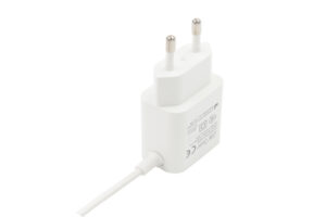
One of the most visible applications of GaN technology today is in fast chargers for consumer electronics like smartphones, tablets, and laptops. I’m sure many of us have noticed how chargers have become smaller yet more powerful over the last few years. GaN is a key reason for this. By using GaN transistors, we manufacturers can design charging devices that are significantly more compact, lighter, and more efficient than traditional silicon-based chargers. I remember getting my first 65W GaN charger; it was barely larger than an old 5W phone charger but could power my laptop! This is a huge convenience for users, especially travelers. For companies like Jacky’s, offering a small, powerful GaN charger as an accessory can be a strong selling point, enhancing the user experience of their primary devices. We’re seeing charging speeds increase and adapter sizes shrink, all thanks to GaN’s capabilities.
Greening Data Centers with GaN?
Data centers are the backbone of our digital world, but they are also massive consumers of energy. Every bit of efficiency in their power delivery systems counts. GaN technology is playing an increasingly important role here. Power supplies using GaN can achieve higher conversion efficiencies, which means less electricity is wasted as heat when converting AC power from the grid to the DC power used by servers. This not only reduces the data center’s overall energy consumption and operational costs but also lessens its environmental impact. Furthermore, the higher power density of GaN-based power supplies can help save valuable space in server racks. Given that Jacky’s company is concerned with global compliance standards like energy efficiency, solutions like GaN-powered data center equipment align perfectly with these sustainability goals.
Powering the Future of Electric Vehicles?
The electric vehicle (EV) market is growing rapidly, and with it, the demand for efficient and fast charging solutions. GaN technology is finding its place in both on-board chargers (OBCs) within the vehicles and off-board DC fast chargers. Compared to traditional silicon-based chargers, GaN chargers can be smaller, lighter, and more efficient. This means faster charging times for EV batteries and less energy loss during the charging process. For on-board chargers, a smaller and lighter unit contributes to better vehicle efficiency and range. For charging station providers, more efficient and compact chargers mean lower installation and operational costs. I believe GaN is a critical enabling technology for making EVs more practical and appealing to a wider audience, contributing to a cleaner transportation future. It’s exciting for us at Quankang to be part of this transition.
| Application Area | Key GaN Benefit Utilized | Impact on Users/Industry |
|---|---|---|
| Smartphone/Laptop Chargers | High frequency, high power density, high efficiency | Smaller, lighter, faster chargers; improved portability |
| Data Center Power | High efficiency, high power density | Reduced energy consumption, lower operating costs, space-saving |
| Electric Vehicle Charging | High efficiency, high power density, thermal performance | Faster charging, smaller/lighter chargers, less energy waste |
Conclusion
GaN transistors truly boost power adapter efficiency and power density. Despite some current cost and thermal challenges, its future is very bright, promising even more compact and powerful solutions.